Thursday, December 20, 2012

Verizon Completes Critical Steps in Bringing Fiber-Optic Connectivity to Lower Manhattan


New Fiber-Optic Infrastructure Will Make NYC Nation's Most Advanced and Robust Communications Center

NEW YORK, Dec. 19, 2012 /PRNewswire/ -- Less than seven weeks after Hurricane Sandy, Verizon has finalized another important step in the transformation of the communications infrastructure of lower Manhattan by completing the installation of fiber-optic cables between the company's two critical central switching offices there and buildings put out of service by the storm surge. 

The completion of the fiber-installation phase of the project – with more than 5,000 miles of fiber strands already in place -- enables Verizon to dramatically modernize communications capabilities for customers as it restores services to the businesses and office buildings in lower Manhattan that were impacted by the hurricane.  Once the project is complete, the area will have the nation's most advanced communications infrastructure, providing customers with the highest level of service and reliability.  Furthermore, the modernization project will make lower Manhattan "future-proof," enabling Verizon to continually update the communications infrastructure with new capabilities for decades to come.

(Note:  To view or download photos of Verizon technicians constructing a telecom room at 55 Water St., installing fiber-optic cables at John and Pearl streets, and a Verizon representative taking FiOS orders in the lobby at 55 Broad St., go to http://vz.to/VNPcQ0.  For additional photos, visit http://vz.to/UaaBH1.)

During the restoration process, Verizon has provided alternate communications solutions to thousands of small businesses and residential customers in the area and elsewhere around the metro area to get them back in business and their communications flowing.  The company has provided call-forwarding capabilities to approximately 7,000 lines of consumers and small businesses so that calls are automatically forwarded to a working landline or cellphone number.  In addition, the company has provided at no charge to customers more than 2,600 Verizon Wireless Home Phone Connect and Verizon 4G LTE Jetpack™ Mobile Hotspot devices.

 While the company has been installing the robust fiber infrastructure, it is also working with landlords as they ready their properties for the return of tenants.  The reconstruction of telecom rooms – frequently relocated to upper floors – power, and access to those rooms are on the critical path to the restoration of communications services. 
 
As building owners and managers complete these steps, Verizon is rapidly completing the work of connecting the newly laid fiber to new electronic systems and turning up service.  The steps these building owners are taking, in conjunction with the new fiber infrastructure from Verizon, will provide additional protection for the communications infrastructure in lower Manhattan in the event of future large-scale weather events.

Verizon continues to operate two command centers in Manhattan where its operations and engineering teams can swiftly design and reconfigure new fiber systems and routes, and then work with building managers to identify space within their structure to locate the new equipment, electronics and cabling.

"The work Verizon is doing now will make us a smarter, faster, better-connected city and region," said Mitchell Moss , Henry Hart Rice Professor of Urban Policy and Planning at New York University.  "These repairs will actually lay the groundwork for a new era of growth and higher efficiency, which will benefit everyone."

5,000 Miles of Fiber Strands Already Installed

The company estimates that more than 70 percent of the affected buildings served by its Broad Street switching office, where copper services were most significantly damaged, have fiber-optic cables and facilities serving them, with many buildings downtown having full service. 

In addition, the company estimates that it has already installed in the dense lower Manhattan area more than 5,000 miles of fiber strands.  Thus far, more than 100 tons of copper cables have been removed from the company's network in the area – 30 percent more than all the copper in the Statue of Liberty.  And more is being removed each day.  The copper is being collected and recycled in an environmentally sensitive process.

"We are doing years' worth of work in just a few weeks' time, and doing it round the clock," said Martin Burvill , senior vice president of global operations for Verizon Enterprise Solutions.  "We are keenly focused on transforming the communications infrastructure of lower Manhattan with this new architecture in a way that fully benefits our residential and business customers. 

"Although this work is being done away from the public's view – in basements, manholes and in still-darkened office towers – it will have a visible and lasting impact by providing a critical part of the city with a network that is world-class, and built for the communications needs of the 21st century," Burvill said.

Verizon has also had an open and continuous dialogue with manufacturers and vendors that supply the industry with electronics necessary to terminate sophisticated fiber networks and the wide range of services they deliver.  The great need for equipment prompted by Hurricane Sandy restoration efforts continues to put pressure on supply chains of specialized equipment, which in turn affects restoration efforts.
 
Copper cables were destroyed that served businesses and residences in the area south of Worth Street, from the East River to the Hudson River.  These cables were rendered inoperable as the result of the unprecedented flooding, the mixture of salt water and diesel fuel in some buildings from compromised tanks that were in place to fuel generators, and the loss of air pressurization systems that help protect copper cables from water infiltration.

Verizon Communications Inc. (NYSE, Nasdaq: VZ), headquartered in New York, is a global leader in delivering broadband and other wireless and wireline communications services to consumer, business, government and wholesale customers.  Verizon Wireless operates America's most reliable wireless network, with nearly 96 million retail customers nationwide.  Verizon also provides converged communications, information and entertainment services over America's most advanced fiber-optic network, and delivers integrated business solutions to customers in more than 150 countries, including all of the Fortune 500.  A Dow 30 company with $111 billion in 2011 revenues, Verizon employs a diverse workforce of 184,500.  For more information, visit www.verizon.com.

VERIZON'S ONLINE NEWS CENTER: Verizon news releases, executive speeches and biographies, media contacts, high-quality video and images, and other information are available at Verizon's News Center on the World Wide Web at www.verizon.com/news.  To receive news releases by email, visit the News Center and register for customized automatic delivery of Verizon news releases.

SOURCE Verizon Communications, Inc.

PR Newswire (http://s.tt/1xq03)
Sunday, September 30, 2012

Product Enhancements - Fiber Optic Fusion Splicer

ENHANCEMENTS TO FITEL® FUSION SPLICER LINE FROM OFS

OFS, a leading designer, manufacturer and supplier of innovative fiber optic network products, has announced a number of product enhancements to its line of FITEL® hand-held fusion splicers.

The upgrades, which include a built-in battery recharger, a selectable display layout, and more user-friendly LCD monitors, further enhance the performance of the company’s S123 Clad Alignment Splicer, the S153 Active Alignment Splicer, and the S178 Core Alignment Splicer.

The built-in battery recharger eliminates the need for carrying a separate external charger into the field. The recharger operates during fusion splicing, with a red icon indicating recharging status.

The selectable display layout enables users to select their preferred display style for viewing the fiber image during the splice operation. Users can choose from a conventional layout, a side-by-side display, and a top-to-bottom comparison, all at the flip of a software switch.

LCD monitors on the FITEL machines have been re-designed to provide even greater visibility while the windshield is open. The opening angle of the windshield has been slightly narrowed with no change to accessibility to the splice chamber.             
 
These product enhancements continue OFS’ tradition as a market leader in the development of ruggedized high-performance splicers for FTTH applications. OFS was first to market with this line of splicers in 2010, and the company believes these product upgrades help enable it to maintain its position as a leading supplier of reliable and intuitive machines for these applications.

The enhancements are the result of consultations with end users, who provided feedback on performance of the machines under real-world conditions, said Linda Dembowski, general manager of the company’s Optical Connectivity Solutions business.

“There is no better source for product improvements than the product’s users,” Dembowski said. “OFS is dedicated to continuous improvement of our splicers based on proven, real-world experience.”

These machines are part of OFS’ full range of rugged hand-held fusion splicers offering speed, durability, and low loss in small, lightweight hand-held design. The machines are designed to endure harsh operating conditions by improving shock/impact resistance with rubber pads embedded on four corners of the splicer body. They also are water resistance-compliant to IPX2 and dust resistance-compliant to IP5X.

About OFS OFS is a world-leading designer, manufacturer and provider of optical fiber, optical fiber cable, connectivity, FTTX and specialty photonics solutions.  Our marketing, sales, manufacturing and research teams provide forward-looking, innovative products and solutions in areas including Telecommunications, Medicine, Industrial Automation, Sensing, Government, Aerospace and Defense applications. We provide reliable, cost effective optical solutions to enable our customers to meet the needs of today’s and tomorrow’s digital and energy consumers and businesses.

OFS’ corporate lineage dates back to 1876 and includes technology powerhouses such as AT&T and Lucent Technologies. Today, OFS is owned by Furukawa Electric, a multi-billion dollar global leader in optical communications.

Headquartered in Norcross (near Atlanta) Georgia, U.S., OFS is a global provider with facilities in China, Denmark, Germany, Russia, and the United States.
For more information, please visit www.ofsoptics.com.

Source Link: http://www.ofsoptics.com/press_room/view_press_release.php?txtID=343

Resonator Fiber Optic Gyroscope (RFOG)

Patent Description - A resonator fiber optic gyroscope (RFOG) is disclosed that reduces rotation rate error instability. In one embodiment, the RFOG comprises a resonator optical ring cavity, a first light source in optical communication with the ring cavity and configured to generate a clockwise optical signal, and a second light source in optical communication with the ring cavity and configured to generate a counter-clockwise optical signal.

The RFOG also includes a first optical component in optical communication with the first light source and the ring cavity. The first optical component is configured to prevent the clockwise optical signal from being back-reflected to the first light source. A second optical component is in optical communication with the second light source and the ring cavity.

See Source Link for complete detail: http://www.google.com/patents/US20120050745

Furukawa - Multi-Core EDFA (Optical Amplifier)

Furukawa Electric Develops Optical Amplifiers for Multi-Core Fibers to Support High Capacity Optical Communications

~ Substantial Energy Savings Achieved by using Collective Excitation to Amplify Signals in Seven-Core Optical Fibers ~

September 20, 2012
Furukawa Electric has developed a multi-core erbium-doped fiber amplifier (MC-EDFA)(Note 1) for use with multi-core optical fibers (MCF)(Note 2) that allow seven optical signals to be input simultaneously. We have also achieved substantial energy-savings for optical amplifiers by developing a collective excitation MC-EDFA using our amplifier technologies and connection mechanisms for optical fibers.

Some of this research has been conducted as part of the Commissioned Research for Advanced Telecommunications and Broadcasting Research and Development sponsored by the National Institute of Information and Communications Technology, specifically the Research and Development of Innovative Optical Fiber Technologies (2010 to 2012) program and Research and the Development of Innovative Optical Telecommunications Infrastructure (2011 to 2015) program.

Research and development relating to multi-core fibers has been conducted jointly with Tohoku University (Nakazawa Laboratory), while research and development relating to MC-EDFAs has been conducted jointly with Tohoku University (Nakazawa Laboratory) and Tohoku Gakuin University (Matsuura Laboratory), and research and development relating to the multi-core fiber connection technologies used within the MC-EDFA has been conducted jointly with the Chiba Institute of Technology (Nagase Laboratory).
Background
The volume of telecommunications data continues to increase all around the world, as the result of the use of smartphones and other factors, and there are concerns that at this rate the number of devices at relay stations will balloon, as well the amount of electricity consumed. Furukawa Electric has developed a new type of optical fiber(Note 1) that enables multiplexing by having seven paths (cores) inside a single fiber, in order to make this kind of high-capacity optical communication possible. Development of optical amplifiers was essential in order to achieve long distance transmissions using this optical fiber.

 
Results announced
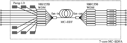
Furukawa Electric has used its optical fiber and amplifier technologies to develop two types of amplifiers: a seven-core EDFA with good regulation properties where each core is excited individually, as well as an MC-EDFA where all cores are excited collectively. The collective excitation MC-EDFA in particular enables substantial energy savings because, unlike traditional amplifiers, it does not require a separate laser for each individual core.

The seven-core individual excitation amplifier inputs the signal beams and excitation beams into an MC-EDF via a fiber bundle fanout (FDF)(Note 3). The behavior of the MC-EDFA has been verified in transmission tests conducted jointly by KDDI R&D Laboratories (hereinafter "KDDI Labs") and NEC Corporation (hereinafter "NEC") using a configuration where 40 waves of 128 Gbps were sent along a 6160 kilometer MCF transmission route. In these demonstrations, the MC-EDFA achieved a world record 177 petabits-per-second.kilometers, a transmission capacity index expressed as the communication capacity multiplied by the transmission distance.

For the collective excitation amplifier, a spaced coupling system was used to input the signal beams and the excitation beam into an MC-EDFA. At present, performance has been verified for the amplification of up to two cores. We have confirmed that there is almost no increase in power consumption even as the number of cores increases, and that the efficiency of electricity usage improves as the number of cores increases.

Example configuration for the item developed

Example configuration for the item developed
Future prospects
Furukawa Electric will carry out fundamental research into areas such as lowering power consumption and increasing the number of cores, in conjunction with initiatives directed at developing practical applications for these technologies, with a view to commercialization after 2020, by which time the volume of telecommunications data is expected to come under pressure.

Of this research, we will present reports about the two types of MC-EDFA at the European Conference on Optical Communication (ECOC) to be held between September 16 and September 20 in Amsterdam in the Netherlands. In addition, we will also present a report at the ECOC Post Deadline Paper Session on the results of the transmission tests that were conducted together with KDDI Labs and NEC.

Notes
(Note 1)Multi-Core Erbium-Doped Fiber Amplifier (MC-EDFA):
An MC-EDFA is a type of EDFA(Note 4) that uses multi-core erbium-doped fibers (MC-EDF), which are optical fibers that contain multiple erbium-doped cores. Multiple optical signals can be amplified using a single MC-EDF, thereby making efficient amplification possible.Back to Main Content

(note 2)Multi-Core Fiber (MCF):
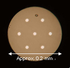
A multi-core fiber is an optical fiber that has multiple paths (cores) for signals. Currently seven-core MCFs are the most prevalent, but there are also reports of MCFs with as many as 19 cores. Because each fiber has multiple cores, there are concerns about interference between cores, but we have confirmed that interference can be constrained by maintaining an optimal distance between cores.Back to Main Content

Photograph showing a cross-section of an MCF

(note 3)Fiber Bundle Fanout (FBF):
An FBF is an optical component that enables all of the cores of an MCF to be connected, by bundling optical fibers that are finer than a normal optical fiber. Using FBFs enables MCFs to be connected to all kinds of optical components. Another feature of FBFs is that they result in less coupling loss than other coupling methods, and there is little reflection, which can be source of interference.Back to Main Content

Illustration of MCF and FBF


(Note 4)Erbium-Doped Fiber Amplifier (EDFA):
An EDFA is an optical amplifier that uses an erbium-doped fiber (EDF) which has been doped with the rare earth element erbium (Er) into an optical fiber. A significant feature of EDFAs is that they have high efficiency with low noise, because by exciting the erbium ion in the EDF with an excitation beam the signal can be amplified without having to convert it to an electrical signal.Back to Main Content


Fujtsu - In-Service Optical Network Resources

Fujitsu Laboratories of America, Inc.
Fujitsu Limited
Fujitsu Develops World's First Technology to Increase Efficiency of In-Service Optical Network Resources
Enables 40% improvement in transmission capacity, accelerates launch of new optical circuits, and cuts energy consumption by eliminating unnecessary network devices

Kawasaki, Japan, Sunnyvale, CA, and Tokyo, September 19, 2012 — Fujitsu Laboratories Limited, Fujitsu Laboratories of America, Inc. and Fujitsu Limited announced the development of the world's first technology for future long-haul and metropolitan optical networks that can dynamically alter the architecture of optical network resources and enhance utilization efficiency without disrupting service. 

As a result of the spread of datacenter-centric cloud services, smartphones and other technologies in recent years, a wide variety of network-enabled services are now being offered. At the same time, for the core networks supporting these services, it is important to be able to shorten the time required to bring online new optical circuits that deliver on-demand services, as well as to increase transmission capacity while reducing the energy consumption of network devices. In light of this, Fujitsu has developed two technologies: "flexible optical node" technology that overcomes limitations in terms of optical signal wavelength, modulation scheme and routes; and "spectrum defragmentation(1) technology," which leverages flexible optical nodes to increase the utilization efficiency of in-service optical network resources. This, in turn, makes it possible to improve optical network transmission capacity by up to 40%.

Using the new technology, optical network architecture can be flexibly altered as needed, and given the improvement in the utilization efficiency of network resources, it is possible to accelerate bringing online new optical circuits while reducing power consumption by eliminating unnecessary network devices.

The digital signal processing LSI employed to test the effectiveness of the new technology was developed as part of Japan's Ministry of Internal Affairs and Communications (MIC)'s project for "R&D on Ultra-High-Speed Optical Transmission Technology."

Background
It seems like every day there are ongoing changes in the ways in which networks are employed, including a variety of applications provided through cloud services, which have expanded primarily thanks to large-scale data centers, and high-speed mobile devices as represented by smartphones, as well as sensor networks and other machine-to-machine (M2M) communications. At the same time, for the core networks supporting these applications, optical fiber network technology has begun to enable the implementation of 100 Gbps/channel-class systems, and in the future, transmission systems achieving greater than 400 Gbps are expected to be available.

In addition to expanding the capacity of such transmission systems, there is a need to offer end-users a variety of flexible network capabilities without having to increase the power consumed by communications nodes and add excess equipment. Such capabilities include offering high-capacity communications routes for on-demand services, the rapid delivery of alternative routes during major natural disasters, and optimal route selection that enables dynamic route reallocation.

Technological Challenges
The following challenges are evident in bringing about the next generation of high-capacity and flexible optical networks.

1. Limitations to the usable spectrum and communications routes of optical networks

Due to the limitations of optical components and electronic components used inside current optical switch nodes and optical transceivers, it is not possible to freely configure the optical wavelengths, bandwidth, modulation schemes and communications routes employed for communications. As a result, to bring new optical circuits into operation, cables have to be manually rerouted and new equipment deployed.

2. Diminished optical wavelength utilization efficiency as a result of in-service adjustments to communications routes

As a result of constantly adjusting optical spectrum routes while a network is in use, fragmentation can occur in the assignment of optical signals that were initially allocated to optimize network utilization efficiency. This spectrum fragmentation makes it impossible to allocate optical fiber communications routes and bandwidth, a process that is necessary to launch new optical circuits, thereby diminishing the utilization efficiency of transmission equipment.

Newly Developed Technology

To address these challenges, Fujitsu has developed technology that can dynamically adjust the architecture of optical network resources and increase utilization efficiency without disrupting service.

1. Flexible optical node (optical transceivers, optical switches) capable of software-side adjustments to network architecture

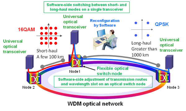
Using digital signal processing technology, Fujitsu developed a "universal transceiver" architecture that makes it possible to make software-side adjustments to the transmission schemes of optical transceivers. To accommodate long-haul users, the nodes can be configured to a relatively wide-band transmission scheme employing a highly noise-tolerant modulation scheme that is suitable for long-haul transmissions. For short-haul users, the nodes can be configured to a transmission scheme that is suitable for short-haul transmissions and features high frequency utilization efficiency, but is not very noise tolerant.

With respect to optical switch nodes, communications bandwidth can be adjusted, and through optical switch technology that enables the selection of multiple communications routes, it is possible to perform software-side configuration of communications routes. Combining these routes enables a single optical switch node to be shared among multiple users, flexible configuration to meet users' needs, and realization of flexible optical nodes that can be configured (Figure 1)
Figure 1: Optical network using flexible optical node technology
2. Improved utilization efficiency of in-service spectrum resources through spectrum defragmentation

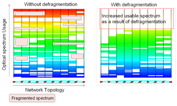
Fujitsu has developed a network control mechanism that employs a defragmentation algorithm for securing usable bandwidth allocable for high-volume data by consolidating fragmented spectrum into an uninterrupted spectrum continuum. Using a flexible optical node device architecture, fragmented optical spectrum resources are continuously consolidated into a wavelength band of a size that is allocable for 400 Gbps-class wide-band signal, all while the network remains in service. By channeling the resulting wavelength band into properly configured optical signals, it is possible to improve the utilization efficiency of spectrum resources.

In an experimental network environment featuring four optical switch nodes, Fujitsu demonstrated—for the first time in the world—the use of defragmentation technology employing digital signal processing technology to shift a 100Gbps DP-QPSK optical signal(2) without disrupting service. By taking advantage of the signal bandwidth made available through the defragmentation process, optical network communications capacity can be improved by 40%.
Figure 2: Results of defragmentation
Results
Using the new technology, optical network architecture can be flexibly altered as needed, and given the improvement in the utilization efficiency of network resources, it is possible to shorten the time required to launch new optical circuits, while cutting power consumption by eliminating unnecessary network devices.

Future Development

Fujitsu will work to standardize 400 Gbps-class next-generation interfaces while developing hardware and pursuing R&D on network management systems in aiming to commercialize the new technology.

Glossary and Notes
Defragmentation:
Just like fragmented storage space on hard disks is consolidated to create larger data space, defragmentation in the case of optical networks is a process of securing usable bandwidth that can be allocated for high-volume data by consolidating fragmented spectrum into an uninterrupted spectrum continuum.
 
DP-QPSK Optical Signal:
Dual-Polarization Quadrature Phase Shift Keying. The effective world standard in modulation and demodulation methods for 100 Gbps optical transmission systems.

About Fujitsu

Fujitsu is the leading Japanese information and communication technology (ICT) company offering a full range of technology products, solutions and services. Over 170,000 Fujitsu people support customers in more than 100 countries. We use our experience and the power of ICT to shape the future of society with our customers. Fujitsu Limited (TSE:6702) reported consolidated revenues of 4.5 trillion yen (US$54 billion) for the fiscal year ended March 31, 2012. For more information, please see http://www.fujitsu.com.

About Fujitsu Laboratories

Founded in 1968 as a wholly owned subsidiary of Fujitsu Limited, Fujitsu Laboratories Limited is one of the premier research centers in the world. With a global network of laboratories in Japan, China, the United States and Europe, the organization conducts a wide range of basic and applied research in the areas of Next-generation Services, Computer Servers, Networks, Electronic Devices and Advanced Materials. For more information, please see: http://jp.fujitsu.com/labs/en.

About Fujitsu Laboratories of America, Inc.

Fujitsu Laboratories of America, Inc. is a wholly owned subsidiary of Fujitsu Laboratories Ltd. (Japan), focusing on research on Internet, interconnect technologies, software development and solutions for several industry verticals. Conducting research in an open environment, it contributes to the global research community and the IT industry. It is headquartered in Sunnyvale, CA.
For more information, please see: www.fla.fujitsu.com


Friday, September 28, 2012

Fiber optic particle plasmon resonance sensor based on plasmonic light scattering interrogation

Abstract

A highly sensitive fiber optic particle plasmon resonance sensor (FO-PPR) is demonstrated for label-free biochemical detection. The sensing strategy relies on interrogating the plasmonic scattering of light from gold nanoparticles on the optical fiber in response to the surrounding refractive index changes or molecular binding events. The refractive index resolution is estimated to be 3.8 × 10⁻⁵ RIU.

The limit of detection for anti-DNP antibody spiked in buffer is 1.2 × 10⁻⁹ g/ml (5.3 pM) by using the DNP-functionalized FO-PPR sensor. The image processing of simultaneously recorded plasmonic scattering photographs at different compartments of the sensor is also demonstrated. Results suggest that the compact sensor can perform multiple independent measurements simultaneously by means of monitoring the plasmonic scattering intensity via photodiodes or a CCD.

The potential of using a combination of different kinds of noble metal nanoparticles with different types of functionalized probes in multiple cascaded detection windows on a single fiber to become an inexpensive and ultrasensitive linear-array sensing platform for higher-throughput biochemical detection is provided.

Notes:
Lin, H.-Y., Huang, C.-H. and Chau, L.-K. (2012), Fiber optic particle plasmon resonance sensor based on plasmonic light scattering interrogation. Ann. Phys.. doi: 10.1002/andp.201200157

Article first published online: 24 SEP 2012
DOI: 10.1002/andp.201200157

SOURCE LINK: http://onlinelibrary.wiley.com/doi/10.1002/andp.201200157/abstract


Calix to Acquire Fiber Access Assets from Ericsson; Companies Sign Global Reseller Agreement


Partnership will bring Calix Unified Access systems and software to communications service providers worldwide

Calix, Inc. (NYSE:CALX) and Ericsson (NASDAQ:ERIC) signed of a definitive agreement under which Calix will acquire Ericsson's fiber access assets. The two companies also announced that they have signed a global reseller agreement, under which Calix will become Ericsson's preferred global partner for broadband access applications.

The acquisition brings together the industry's highest capacity GPON solution, deployed by major service providers worldwide, with North America's leading access portfolio. Ericsson's fiber access assets expected to be included are the Ericsson EDA 1500 GPON solution and its complementary ONT portfolio. The agreement also calls for Calix to offer employment for up to 61 U.S.-based employees of Ericsson, as well as the transition of ongoing support of the acquired products from Ericsson to Calix. The acquisition transaction is expected to close in the fourth quarter of 2012. Financial terms of the transaction were not disclosed. After close of the transaction, Calix expects operations related to the acquired assets to be accretive to non-GAAP earnings per share.

The global reseller agreement between the two companies allows Ericsson to sell Calix Unified Access systems and software as its preferred fiber and VDSL2 access solution in 180 countries worldwide. This preferred partnership becomes effective upon the close of the acquisition and remains effective for three years.

"This partnership provides Calix, already North America's fiber access deployment leader, with an extensive new global reseller channel, while our acquisition of Ericsson's fiber access portfolio delivers powerful new complements to our industry-leading Unified Access portfolio," said Carl Russo, president and CEO of Calix. "This partnership, built on a clear alignment of corporate strategy and direction, allows Ericsson to fully leverage its strengths in wireless and end-to-end services while relying on Calix to provide innovation and expertise in fixed-line broadband access. We are excited about the opportunity to assume responsibility for development and support of Ericsson's fiber access business, and look forward to working closely with Ericsson and its broad customer base as a preferred global partner."

"We believe that this partnership will provide our existing fiber access customers with world-class support and maintenance, and an expanded portfolio of access systems and software from a leading company totally focused on access," said Jan Häglund, vice president and head of product area IP and broadband at Ericsson.

About Calix
Calix (NYSE: CALX) is a global leader in access innovation. Its Unified Access portfolio of broadband communications access systems and software enables communications service providers worldwide to be the broadband provider of choice to their subscribers. For more information, visit the Calix website at http://www.calix.com/.

About Ericsson
Ericsson is the world's leading provider of communications technology and services. We are enabling the Networked Society with efficient real-time solutions that allow us all to study, work and live our lives more freely, in sustainable societies around the world.
Our offering comprises services, software and infrastructure within Information and Communications Technology for telecom operators and other industries. Today more than 40 percent of the world's mobile traffic goes through Ericsson networks and we support customers' networks servicing more than 2.5 billion subscribers.
We operate in 180 countries and employ more than 100,000 people. Founded in 1876, Ericsson is headquartered in Stockholm, Sweden. In 2011 the company had revenues of SEK 226.9 billion (USD 35.0 billion). Ericsson is listed on NASDAQ OMX, Stockholm and NASDAQ, New York stock exchanges.

OTDR-Based Remote Test Unit for Automated FTTH Fault Management

QUEBEC CITY, CANADA, September 25, 2012 — EXFO Inc. (NASDAQ: EXFO) (TSX: EXF) announced today new additions to its Fiber Guardian product family, including the FG-750 Node iOLM, a specialized OTDR designed for in-service FTTH fiber testing, monitoring and troubleshooting. This latest EXFO innovation can test point-to-multipoint fibers, or run downstream tests from the node or central office to any passive optical network line type, providing operators with an automated, operation-oriented way of assessing the health of their FTTH networks.

The need for optical demarcation in FTTH networksOpen FTTH network and multitenant environments require establishing a clear responsibility boundary between the operator and the service provider, even at the optical fiber layer. Also, limited access to customer premises and longer commuting times in cities and urban areas put increased pressure on operating costs and the importance of reducing truck rolls. Finally, added to these aspects is this everyday challenge: efficiently testing quality and continuity between a network node, point of presence (PoP), central office or exchange site and a customer premises.
Addressing the challengeBased on EXFO’s patented Link-Aware technology, the Node intelligent Optical Link Mapper (iOLM) allows operators to monitor and validate end-to-end fiber quality from a centralized location, and throughout the lifecycle. Its ability to perform online quality control of contractual work, and to further use the same equipment for isolating and pinpointing optical-layer impairments in a more automated way is expected to significantly increase operational efficiency.

Its carrier-class hardware meets FTTx network requirements such as connection to a multiple optical test ports, use of multifiber cables (MFCs), low power consumption, small volume and scalability. In addition, EXFO is introducing cost-efficient 576-port and 720-port optical switch and test access modules allowing in-service addition of out-of-band OTDR signals to the line under test, all from the node. In terms of software, the connectivity and access to the test platform is provided through a full set of representational state transfer (REST) services (APIs) allowing easy integration by virtually any system integrator, network equipment manufacturer or tier-1 operator.

“After having launched the Ethernet One solution, which allows to deploy and assure Carrier Ethernet services more cost-effectively, we are proud to reinforce our commitment to providing our customers with productivity-boosting tools that can shorten the on-field assessment cycles and time-to-revenue,” said Étienne Gagnon, Vice-President of EXFO’s Test and Measurement Division. “When used in a support and maintenance environment, the Node iOLM allows operators to monitor and validate end-to-end fiber quality from a centralized location, and throughout the network lifecycle.”

Visit the EXFO Link for more on the FG-750 Node iOLM.

About EXFO
Listed on the NASDAQ and TSX stock exchanges, EXFO is among the leading providers of next-generation test and service assurance solutions for wireline and wireless network operators and equipment manufacturers in the global telecommunications industry. The company offers innovative solutions for the development, installation, management and maintenance of converged, IP fixed and mobile networks—from the core to the edge. Key technologies supported include 3G, 4G/LTE, IMS, Ethernet, OTN, FTTx, VDSL2, ADSL2+ and various optical technologies (accounting for an estimated 35% of the portable fiber-optic test market). EXFO has a staff of approximately 1800 people in 25 countries, supporting more than 2000 telecom customers worldwide. For more information, visit www.EXFO.com.

EXFO Brand Name
The corporate name of the company is EXFO Inc. The company requests that all media outlets and publications use the corporate name (“EXFO Inc.”) or abbreviated name (“EXFO”) in capital letters for branding purposes. EXFO would like to thank all parties in advance for their cooperation.

Wednesday, September 12, 2012

Photonic Switch - Venture Capital

CrossFiber Completes $13.4 Million Series D Financing
Southern Cross Venture Partners led the round, with participation from New Venture Partners, Arsenal Venture Partners and existing investors including Back Bay Management and PacifiCap. Provide Expansion Capital for Photonic Switch Maker

September 12, 2012, San Diego, California --CrossFiber Inc., the developer and manufacturer of breakthrough photonic switches that enable novel architectures in data centers and next-generation telco fiber optic networks, announced today the completion of the final tranche of its Series D funding, now totaling $13.4 million. The Company said that the majority of the funds have been and will continue to be used for rapid expansion of manufacturing capacity, to meet the high demand for LiteSwitch™ family of photonic switches. Southern Cross Venture Partners led the round, with participation from New Venture Partners, Arsenal Venture Partners and existing investors including Back Bay Management and PacifiCap.

"With unique technologies and products attracting tier-one customers, CrossFiber is leading the way in optical switching in data centers and telecommunications. We are delighted to be a part of CrossFiber's exciting story, and to work alongside such great domain expert investors as NVP, Arsenal, Back Bay, Trex, and PacifiCap," said Dr. Larry Marshall, Managing Director of Southern Cross. "We welcome the new investors in this rapid-growth stage of the company and thank all investors for their confidence and support," said Hus Tigli, President & CEO of CrossFiber.

About CrossFiber
CrossFiber develops and manufactures breakthrough photonic switches, based on proprietary technologies which combine 3D MEMS micro-mirrors on silicon, non-invasive beam steering (NIBS), and custom ASICs. CrossFiber's unique combination of performance and cost makes LiteSwitch™ systems the most suitable across all major applications in data centers and telco fiber optic switching. More information can be found at www.crossfiber.com.

Fiber Optic Submarine Line: 70 x 100G capacity per fiber pair

Tamares Telecom, the provider of new international communications from and to Israel, and Xtera Communications Inc. (Xtera), a leading global provider of optical networking solutions, announce that the Tamares Telecom network providing seamless connectivity from Israel to international communication hubs in Europe is now fully operational.  For this innovative project, Xtera supplied its advanced, multi-purpose and field-proven Nu-Wave OptimaTM platform deployed in a Submarine Line Terminal Equipment (SLTE) configuration with 70 x 100G capacity per fiber pair.  Xtera partnered with IT International Telecom (IT), a subsea network integrator, to provide Tamares Telecom with a turnkey solution including supply and installation of both transmission equipment and cable.
Tamares Telecom is a communications service provider that operates and markets communication services, paving the way for faster and more reliable internet access.  The new fiber optic network, including a new submarine cable connecting Israel to Marseille and from Marseille to Frankfurt and London, is designed to provide a secure, high speed connection for data traffic moving east and west for international carriers.
"This region has experienced explosive growth in traffic from the local high tech boom as well as R&D centers of global giants including IBM, Microsoft, Google, Apple, Intel, and Motorola," said Amir Goldstein, Executive Vice Chairman of Tamares Telecom.  "We are happy to work with Xtera & IT's cutting edge technology that enables our network to provide carriers and enterprises with confidence in the quality and security of their international connections."
Xtera’s Nu-Wave OptimaTM platform is a unique modular optical transport system designed to lower the total cost of ownership by using a common, integrated set of modules for long-haul, unrepeatered and regional repeatered submarine applications.
Being the first and only 100G equipment in the field since the second half of 2011 with soft-decision Forward Error Correction (FEC), Xtera’s Nu-Wave OptimaTM offers the industry’s most advanced 100G solution that is available for multiple optical networking applications.  For terrestrial backbone networks, the Nu-Wave OptimaTM equipment delivers an unrivalled line capacity of 15 Tb/s on more than 3,000 km.  For unrepeatered applications, a capacity of 34 x 100G was recently transmitted over a cable attenuation exceeding 74 dB.
“Xtera is extremely pleased to be part, once again, of a new international submarine cable system project.  This is a further example of how Xtera’s advanced technologies can benefit high-capacity networks for bandwidth-intensive services,” said Jon Hopper, President and CEO of Xtera.
The proven Nu-Wave OptimaTM multi-purpose platform offers unparalleled 100G WDM performance in real network conditions based on the combination of the industry’s most powerful 100G technology and unique line equipment to face different span configurations.  Some examples include:
·         A N x 100G 1,350-km route including a 250-km / 60-dB span;
·         The longest N x 100G all-optical link ever deployed with a reach of 2,500 km, including 24 spans, and going through 9 ROADMS; and
·         7 Tb/s per fiber pair on a 350-km / 65.5-dB unrepeatered link.
In addition to unrivalled transmission performance, the Nu-Wave OptimaTM platform achieved the following industry’s firsts:
·         First soft-decision FEC in the field in 2011;
·         World’s widest 100G deployment (CFE Telecom’s 22,000-km backbone network in 2011); and
·         First 100G repeatered subsea cable system to be put in commercial service (first quarter of 2012).

About Tamares Telecom
Tamares Telecom is a privately held service provider that operates and markets communications services based on a new internationally deployed fiber-optic network. Tamares Telecom provides seamless connectivity from Israel to international communications hubs and enhances the value it brings to its customers with innovative, fast, reliable and cost-effective solutions and services that address today’s and tomorrow’s challenges. Moreover, the company has joined forces with world-leading technology vendors and business partners.  Tamares Telecom is part of Tamares Group.  For more information, visit www.tamarestelecom.com.

About Xtera Communications, Inc.
Xtera Communications, Inc. (Xtera) specializes in network infrastructure that delivers maximum capacity, reach and value.  Providing solutions for enterprise and telecom companies, Xtera offers an extensive portfolio of optical and IP networking solutions for submarine, long-haul, regional and enterprise applications.  With deployments across five continents, Xtera’s optical transport solutions help service providers expand and accelerate their market reach with new deployments and extend the life of existing network assets with cost-effective upgrades.  Our IP networking solutions for WAN traffic management deliver efficient, flexible network optimization.  Xtera’s innovative technologies offer exceptional quality and performance, driving customer success.  For more information, visit www.xtera.com.

About IT International Telecom
IT International Telecom is an innovative company proud to provide its clients with customized solutions that meet their telecommunication, power installation and maintenance requirements.  IT International Telecom is ISO 9000-2001 certified and has provided network installations in more than 65 countries and counting.  IT has offices in Montreal, Canada and Bridgetown, Barbados as well as marine depots in Campbell River and Halifax, Canada.  For more information, please visit www.ittelecom.com

SOURCE LINK:   http://www.xtera.com/news/83


Monday, September 10, 2012

FTTH - Country Cablevision expects to begin turning up fiber service in early 2013

Country Cablevision has begun deploying Clearfield’s FieldSmart Fiber Scalability Center (FSC) as part of its fiber-optic broadband network build.

Country Cablevision, which provides services in rural Mitchell and Yancey counties in N.C., is among the first cable companies to pursue a full fiber-to-the-home (FTTH) strategy. The company is using $25.3 million from the U.S. Department of Agriculture’s Rural Utilities Service (RUS) to provide high-speed Internet services to more than 33,000 people, 1,900 local businesses and 120 community institutions.

As part of the deployment, Country Cablevision plans to place more than 100 FieldSmart FSC 288 PON Cabinets throughout its service area. Through the incremental design, capacity can be scaled to the maximum configuration of the cabinet, allowing Country Cablevision to align the investment in capital equipment to the turn-up of revenue-generating circuits.

"With this project, we reviewed several architectures and had many options for housing our optical splitters and fiber terminations," said Randall Miller, president of Country Cablevision. "We selected Clearfield's FieldSmart Fiber Scalability Center, as it provides a centralized point from which we can serve hundreds of customers. The Clearfield cabinet offers the best fiber protection, access and management in the industry, which will allow us to maintain a state-of-the-art network for many years to come."

The project is underway, and Country Cablevision expects to begin turning up fiber service in early 2013.

Cheri Beranek, president and CEO of Clearfield, said, "While the traditional hybrid fiber/coax (HFC) network has served the cable TV community well, the emergence of FTTH networks in the multiple service operator space demonstrates the immediate and long-term economic opportunity of a rich fiber network."

Saturday, September 1, 2012

US IGNITE - broadband infrastructure projects

The President of the United States recently signed an Executive Order (EO) to make broadband construction along Federal roadways and properties up to 90 percent cheaper and more efficient.

         Currently, the procedures for approving broadband infrastructure projects on properties controlled or managed by the Federal Government—including large tracts of land, roadways, and more than 10,000 buildings across the Nation—vary depending on which agency manages the property. The new Executive Order will ensure that agencies charged with managing Federal properties and roads take specific steps to adopt a uniform approach for allowing broadband carriers to build networks on and through those assets and speed the delivery of connectivity to communities, businesses, and schools.

         The White House also announced that nearly 100 partners—including more than 25 cities as well as corporate and non-profit entities—will join with more than 60 national research universities to form a new public-private partnership called “US Ignite.” The US Ignite Partnership will create a new wave of services that take advantage of state-of-the-art, programmable broadband networks running up to 100 times faster than today’s Internet. By bringing software developers and engineers from government and industry together with representatives from communities, schools, hospitals, and other institutions that will benefit from faster and more agile broadband options, the partnership aims to speed up and increase the development of applications for advanced manufacturing, medical monitoring, emergency preparedness, and a host of other services. These applications will improve services to Americans and drive job creation, promote innovation, and create new markets for American businesses.

         Executive Order           The Executive Order (EO) requires the Departments of Agriculture, Commerce, Defense, Interior, Transportation, and Veterans Affairs as well as the US Postal Service to offer carriers a single approach to leasing Federal assets for broadband deployment. The EO also requires available Federal assets and the requirements for leasing is provided on departmental websites, and it will require public tracking of regional broadband deployment projects via the Federal Infrastructure Projects Dashboard (permits.performance.gov). In addition, the Executive Order directs departments to help carriers time their broadband deployment activities to periods when streets are already under construction—an approach that can reduce network deployment costs along Federal roadways by up to 90 percent.

         Industry partners offer support to partnership: Global industry leaders including Cisco, Juniper, NEC, and Hewlett-Packard are offering programmatic and in-kind support to communities while carriers, like Verizon and Comcast, are announcing new pilot cities on their network that will participate in US Ignite.

         New tools for communities: Non-profits, like the Mott Foundation, are working with the partnership to deliver new community programs, such as hack days and startup weekends, to accelerate the transition these applications into the marketplace.

         National coalition of universities: The National Science Foundation (NSF) is committing $20 million to prototype and deploy new technologies to advance the development of ultra-high-speed, programmable broadband networks. That is in addition to the ~$40 million that NSF has invested over four years in the Global Environment for Networking Innovations (GENI) project, which currently connects more than a dozen universities with next-generation broadband connections. Built with the technological contributions of more than 300 NSF-funded researchers at more than 60 universities, GENI is already serving as a virtual laboratory and testbed for next-generation applications in healthcare, energy efficiency, education, and other national priority areas.

         Next-Gen apps challenge to spur innovation: NSF and Mozilla Foundation, with support from the Department of Energy, are announcing a $500,000 design competition to develop applications for high-speed communities around the country.

         Building on current broadband investments: Departments of Commerce and Agriculture are announcing their support for US Ignite with over six carriers that received funding for expanding their broadband networks while creating new community-based services.
         Supporting military families and communities with new applications: Department of Defense is connecting military families on base with new US Ignite services, while creating new research opportunities to students at West Point. HHS’s Beacon Community Program, starting with the Mayo Clinic, and the Federal Communications Commission’s Rural Healthcare Pilot Program are partnering with US Ignite to provide new healthcare applications, such as remote surgical theatre and patient monitoring.

Broadband deployment programs already underway include:

NTIA’s Recovery Act projects are increasing broadband access in communities across the country, with more than 56,000 miles of networks providing broadband access to more than 8,000 schools, libraries, hospitals, and public safety entities.

USDA’s Rural Utilities Service is currently on target to complete over $3 billion in Recovery Act investments ensuring that rural communities and anchor institutions are connected to high-speed broadband networks.

Friday, August 31, 2012

Fujitsu Laboratories Develops Integrated Silicon Optical Transmitter

- Demonstrates high-speed operation by integrating light source and
optical modulator on the same silicon chip using structure that
obviates need for thermal control mechanism -

Kawasaki, Japan, August 31, 2012 - Fujitsu Laboratories Limited
today announced the development of an integrated silicon optical
transmitter for use in an optical transceiver(1), which is essential
for enabling large volumes of data to be transmitted between CPUs.

Thermal fluctuations from the heat emitted by CPUs have a large
impact on both the light source built into optical transmitters
located near CPUs and the optical modulators(2) that encode data
into the light emitted from the light source. This means a thermal
control mechanism has been required to ensure that the operating
wavelengths of both the light source and optical modulator
consistently match. Fujitsu Laboratories previously devised a
structure incorporating both the light source and optical modulator
that did not require thermal control and demonstrated identical
thermal properties by using separate prototypes of the light source
and the optical modulator. This time, using the same structure to
make a prototype optical transmitter that integrates the light source
and optical modulator on the same silicon chip, Fujitsu Laboratories
demonstrated that it could achieve optical modulation signals at
speeds of 10 Gbps at temperatures ranging from 25 degrees celsius to
60 degrees celsius without a thermal control mechanism. Moreover,
the overall electricity consumed by the optical transmitter was
reduced by roughly half compared to previous methods.

This technology enables compact, low-power optical transceivers
to be mounted directly in CPU packaging. Through its application
exaflops-class supercomputers(3) and high-end servers requiring
high-speed transmission of large volumes of data, the technology
paves the way for super-high-speed computers.

<Background>
In recent years, supercomputer performance has been roughly
doubling every 18 months. Right now, work is underway to produce
exaflops-class supercomputers with a target date around 2020. The
creation of these ultrafast computers will require high-volume data
transmission technology that allows individual CPUs to transfer data
to each other at tens of terabits per second. With existing
electrical interconnects based on copper wire, however, the dramatic
increases required in circuit space, number of transmission lines,
and electricity consumption in accordance with the higher data volumes
are thought to make it difficult to achieve the data transmission
speeds needed for exaflops-class supercomputers. As a result,
consideration is being given to the use of optical interconnect
technology in which, as shown in figure 1, CPUs are connected using
light. Recently, in particular, attention is being focused on the
development of silicon photonics(4) technology enabling optical
transceivers to be compact and densely integrated, and that enables
integration of electrical and optical components.

<Technological Issues>
The transmitter component of an optical transceiver comprises a
light source and an optical modulator that encodes data into the light
emitted by the light source. A good candidate for the optical modulator
is a ring resonator(5), as it is compact and energy efficient. But
because the optical transceiver is located near the CPU, the lasing
wavelength and the operating wavelength of the ring-resonator-based
optical modulator do not coincide with each other due to heat from the
CPU, resulting in information not being encoded in the light. A
thermal control mechanism is needed to ensure that they match exactly,
which, however, is an obstacle to making the transceiver compact and
energy efficient.

<Resolution Approach>
By using the same ring resonator for both the wavelength control unit
of the light source and the optical modulator, Fujitsu Laboratories
previously devised a structure that made the wavelengths of the light
source and optical modulator identical without the need for a thermal
control mechanism. It used this structure to build separate prototypes
of the light source and optical modulator, and it previously
demonstrated that their thermal properties were identical.

<Newly Developed Technology>
This time Fujitsu Laboratories made a prototype optical transmitter
that integrates on the same silicon chip a light source and optical
modulator employing the previously devised structure. Using this
transmitter, it demonstrated that it could make the wavelengths of
the light source and optical modulator identical without the need
for a thermal control mechanism and could achieve optical modulation
signals at speeds of 10 Gbps at temperatures ranging from 25 degrees
celsius to 60 degrees celsius.

Figure 2 depicts the prototype silicon optical transmitter that
integrates the light source and optical modulator. To enable shifts
in the wavelengths caused by temperature changes to match, the same
ring resonator is used for both the wavelength control unit of the
light source and the optical modulator. Moreover, to safeguard
operation even if there are slight differences in the wavelengths of
the light source and optical modulator, the optical modulator is
structured with an alignment of multiple ring resonators, increasing
the operating wavelength range. Using this structure, there is no
need for a thermal control mechanism, and the overall electricity
consumed by the optical transmitter was reduced by roughly half
compared to previous methods. It is compact, measuring roughly only
2 mm long without the semiconductor optical amplifier. Through
optimization using the silicon wire optical waveguide structure(6),
it is expected that in the future the size can be reduced to under
1 mm.

Figure 3 depicts the optical modulation signals measured at speeds
of 10 Gbps at varying temperatures. When varying the temperature from
25 degrees celsius to 60 degrees celsius, the spectrum's peak wavelength
moves to the long-wavelength side, but a stable modulation signal is
derived without controlling the wavelengths.

By further increasing the speed of this optical transmitter and
integrating multiple transmitters on one chip using wavelength
multiplexing technology, it will be possible to create optical transmitters
small enough to be embedded into CPU modules capable of transmitting
large volumes of data at rates of several terabits per second.

<Results>
The use of this technology enables the development of exaflops-class
supercomputers and high-end servers requiring energy efficient
transmission of large volumes of data between CPUs, thereby paving the
way for super-high-speed computers.

<Future Plans>
Fujitsu Laboratories plans to continue development of the optical
receiver using the same silicon photonics technology, and will integrate
it and this new transmitter to create a compact optical transceiver.
Moreover, by applying wavelength multiplexing technology and pursuing
dense integration, it will work on developing large-capacity integrated
optical interconnects capable of enabling data transmission speeds of
tens of terabits per second.

<Glossary and Notes>
1 Optical transceiver:
A module that converts an electrical signal to an optical signal, which
it then transmits, and that also receives an optical signal and converts
to an electrical signal.

2 Optical modulator:
An optical component that converts electrical signals to optical
signals. These include intensity modulators that convert to an
optical-intensity signal and phase modulators that convert to light-phase
signals.

3 Exaflops-class supercomputer:
A supercomputer that can process 10 to the18th "FLoating-point number
Operations Per Second."

4 Silicon photonics:
Technology in which a photonic device is configured on a silicon
substrate. By using silicon, the optical circuits can be made smaller,
enabling dense integration. It also has other merits, such as the
ability to configure optical circuits and electrical circuits in one
unit, and lower manufacturing costs.

5 Ring resonator:
A resonator made of a ring-type optical waveguide. When used in
silicon photonics, this can be made extremely small, with a radius on
the order of microns. The ring's resonance effect makes it possible to
create a highly efficient optical modulator.

6 Silicon wire optical waveguide structure:
An extremely small silicon optical waveguide, in which the height and
width of the cross-sectional surface is less than 1 micrometer.

<About Fujitsu>
Fujitsu is the leading Japanese information and communication technology (ICT)
company offering a full range of technology products, solutions and services.
Over 170,000 Fujitsu people support customers in more than 100 countries. We
use our experience and the power of ICT to shape the future of society with
our customers. Fujitsu Limited (TSE:6702) reported consolidated revenues of
4.5 trillion yen (US$55 billion) for the fiscal year ended March 31, 2011.
For more information, please see http://www.fujitsu.com.

<About Fujitsu Laboratories>
Founded in 1968 as a wholly owned subsidiary of Fujitsu Limited,
Fujitsu Laboratories Limited is one of the premier research centers in the
world. With a global network of laboratories in Japan, China, the United States
and Europe, the organization conducts a wide range of basic and applied
research in the areas of Next-generation Services, Computer Servers, Networks,
Electronic Devices and Advanced Materials. For more information,
please see: http://jp.fujitsu.com/labs/en.

<Press Contacts>
Fujitsu Limited
Public and Investor Relations Division
Inquiries: https://www-s.fujitsu.com/global/news/contacts/inquiries/index.html

<Technical Contacts>
Fujitsu Laboratories Ltd.
Next-Generation Manufacturing Technologies Research Center
E-mail: si-photonics-2@ml.labs.fujitsu.com


Tuesday, August 14, 2012

MRV Announces Conclusion of Exploration of Strategic Alternatives

Aug 10, 2012 (Marketwire via COMTEX) --MRV Communications, Inc. (PINKSHEETS: MRVC) ("MRV" or the "Company"), a leading provider of optical communications network infrastructure equipment and integration and managed services, today announced the conclusion of its previously announced exploration of strategic alternatives.

MRV has determined to divest its Network Integration businesses and retain, build and invest in its core Optical Communications Systems ("OCS") business.

The long-term growth prospects for the optical transport and carrier Ethernet markets reinforce MRV's decision to build its OCS business. MRV's OCS products are well positioned in the marketplace and are known for their rich feature set, for their ability to improve the efficiency of their customers' networks, and for the industry-leading bandwidth to power consumption ratio of its products.

"After a careful and thorough review of our businesses and the markets we serve, the management team and Board of Directors determined that the best course of action for MRV is to pursue divestiture of our Network Integration subsidiaries in Europe and retain and expand our OCS business," said Barry Gorsun, chief executive officer of MRV.

"During our strategic review process, it became very apparent that there is real value in the OCS technology platform and that we are well positioned in the optical transport and carrier Ethernet markets and specifically in the rapidly growing mobile backhaul data center and cloud computing verticals. We believe that we could best serve our stockholders and customers by leveraging these strengths to deliver innovative new products to the high growth segments of our markets. This decision was reinforced by a top tier service provider who recently selected MRV's OptiSwitch® and ProVision® solutions for an international metro-Ethernet deployment. In fact, we have already started shipping against this contract."

Gorsun continued, "Rising demand for bandwidth intensive applications, mobility and cloud computing are the catalysts forcing carriers to upgrade their infrastructure to next-generation networks. Recent market data estimates that the subsets of these markets that MRV addresses are poised for solid long-term growth, despite the current challenging macroeconomic spending environment. Service providers around the globe have come to expect best-in-class products and services from MRV and we intend to build upon this tradition to drive growth and increase our market share over the long term."

For over 20 years, MRV has been providing innovative and award winning solutions to the market. MRV's OCS division is an end-to-end provider of optical communications network infrastructure equipment that facilitates access, transport, aggregation and management of voice, data and video traffic in networks, data centers and laboratories used by telecommunications service providers, cable operators, enterprise customers and governments worldwide.

MRV's OCS division serves the optical transport and carrier Ethernet markets for telecommunications service providers and large enterprises around the globe from the edge to the core of the network. Infonetics Research, Inc. forecasts that the optical transport and carrier Ethernet markets will grow at a compound annual growth rate of 12 percent and 6 percent, respectively, through 2016. These markets are being driven by the proliferation of network traffic due to the increase in 4G mobile network upgrades, cloud computing, data center services, business services, wholesale exchanges, and the systematic conversion to packet-based networks as operators attempt to fill the ever-increasing demand for bandwidth and complex services.

MRV's award winning product families include the OptiSwitch carrier Ethernet, FiberDriver® and LambdaDriver® optical transport, ProVision element management system and MCC and LX infrastructure management solutions. 

As set forth in MRV's preliminary proxy statement filed on Schedule 14A with the Securities and Exchange Commission ("SEC") on August 9, 2012, the Company is seeking stockholder approval for two transactions in the Company's Network Integration business. The Company has entered into a sale purchase agreement for the sale of its French subsidiary, Interdata, and it has entered into a letter of intent which anticipates a potential sale of its Swedish subsidiary, Alcadon-MRV AB. MRV has also retained the investment bank Headwaters BD, LLC, to evaluate and explore strategic alternatives for its Italian subsidiary, Tecnonet S.p.A. A detailed discussion of MRV's proposed sale of Interdata and Alcadon can be found in its preliminary proxy statement on file with the SEC.

About MRV Communications, Inc.
MRV Communications, Inc. is a leading global provider of carrier Ethernet, wavelength division multiplexing optical transport, infrastructure management equipment and solutions, as well as network integration and managed services. MRV's solutions enable the delivery and provisioning of next-generation optical transport and carrier Ethernet services over any fiber infrastructure. MRV provides equipment and services worldwide to telecommunications service providers, enterprises, and governments, enabling network evolution and increasing efficiency, while reducing complexity and costs. Through its subsidiaries, MRV operates development centers in North America and Europe, along with support centers and sales offices around the world. For more information about MRV, visit http://www.mrv.com.

Handheld Fiber Optic OTDR Performs well in Harsh Environments

This handheld fiber optic OTDR is specially designed for fiber network construction and maintenance in FTTx, WAN and CATV systems.

Toronto, Canada – GAO Tek Inc. is offering its portable handheld fiber optic OTDR. This innovative test instrument for telecommunication networks is specially designed for fiber network construction and maintenance in FTTx, WAN and CATV systems.

This handheld fiber optic OTDR, model C0250001, features a compact size, easy operation, high dynamic range and highly precise measurement. It can be used in both single mode (1310/1550 nm) and multi mode (850/1300 nm) fiber applications. The unique hot key design makes it convenient and quick to conduct measurements and review and analyze test results. It is complete with adaptors for connection to different fiber types. It is also resistant to dust, moisture and shock, which allows it to perform well even in harsh environments.

This fiber optic OTDR provides a wavelength of 1310/1550 nm ± 20 nm for single mode fiber and 850/1300 nm ± 20 nm for multi mode fiber. The event dead zone for single mode fiber is only 3 m and for multi mode fiber is 7 m. It has a large memory capacity allowing it to save up to 300 test curves and can transfer them to a computer via RS-232 or USB port for further analysis, reporting and printing via included software. In addition, it is powered by Ni-MH rechargeable battery or AC adapter for over 3.5 hours of continuous testing operation on a single charge.

This handheld fiber optic OTDR belongs to GAO’s family of OTDRs. Two other products in this line are Multi-function Optical Time Domain Reflectometer which is used for testing in a variety of fiber optic applications including WDM, MAN, FTTH and LAN networks, and Handheld Fiber Optic OTDR which features an extra-short event dead zone of only 1.6 m, a high resolution of 0.125 m, 65 k sampling points and a convenient visible fault location (VFL) function.

About GAO Tek Inc.
GAO Tek Inc. specializes in researching, developing, manufacturing and selling top quality and cost effective telecom testers, electrical testers, embedded development tools, RFID readers and tags and other electronic measurement instruments.

Thursday, August 9, 2012

BELLA Laser Achieves World Record

As Berkeley Lab’s laser plasma accelerator project BELLA nears completion, its drive laser has delivered one petawatt – a quadrillion watts – of peak power once each second, a world record for laser performance

The BELLA laser under construction. In the foreground, units of the front end stretch and amplify short, relatively weak laser pulses before further amplification in the long central chamber. Amplification is done by titanium sapphire crystals boosted by a dozen pump lasers. At the far end of the hall the now highly energetic stretched pulse is compressed before being directed to BELLA’s electron-beam accelerator component. (Photo Roy Kaltschmidt, Lawrence Berkeley National Laboratory)
The BELLA laser during construction. In the foreground, units of the front end stretch and amplify short, relatively weak laser pulses before further amplification in the long central chamber. Amplification is done by titanium sapphire crystals boosted by a dozen pump lasers. At the far end of the hall the now highly energetic stretched pulse is compressed before being directed to BELLA’s electron-beam accelerator component. (Photo Roy Kaltschmidt, Lawrence Berkeley National Laboratory)
 
 
On the night of July 20, 2012, the laser system of the Berkeley Lab Laser Accelerator (BELLA), which is nearing completion at the U.S. Department of Energy’s Lawrence Berkeley National Laboratory (Berkeley Lab), delivered a petawatt of power in a pulse just 40 femtoseconds long at a pulse rate of one hertz – one pulse every second. A petawatt is 1015 watts, a quadrillion watts, and a femtosecond is 10-15 second, a quadrillionth of a second. No other laser system has achieved this peak power at this rapid pulse rate. “This represents a new world record,” said Wim Leemans of Berkeley Lab’s Accelerator and Fusion Research Division (AFRD) when announcing the late-night success to his team. Leemans heads AFRD’s Lasers and Optical Accelerator Systems Integrated Studies program (LOASIS) and conceived BELLA in 2006.

“My congratulations to the BELLA team for this early mark of success,” said Berkeley Lab Director Paul Alivisatos. “This is encouraging progress toward a future generation of smaller and far more efficient accelerators to maintain our nation’s leadership in the tools of basic science.”

“Congratulations to all of you on this spectacular achievement,” said Stephen Gourlay, Director of AFRD. “It doesn’t seem that long ago that BELLA was just a dream, and now there is even more to look forward to. Thank you all for the hard work and support that made this a reality.”

Leemans says, “BELLA will be an exceptional tool for advancing the physics of laser and matter interactions. The laser’s peak power will give us access to new regimes, such as developing compact particle accelerators for high-energy physics, and tabletop free electron lasers for investigating materials and biological systems. As we investigate these new regimes, the laser’s repetition rate of one pulse per second will allow us to do ‘science with error bars’ – repeated experiments within a reasonable time.”

The BELLA design draws on years of laser plasma accelerator research conducted by LOASIS. Unlike conventional accelerators that use modulated electric fields to accelerate charged particles such as protons and electrons, laser plasma accelerators generate waves of electron density that move through a plasma, using laser beams to either heat and drill through a plume of gas or driving through plasma enclosed in a thin capillary in a crystalline block like sapphire. The waves trap some of the plasma’s free electrons and accelerate them to very high energies within very short lengths, as if the accelerated electrons were surfing on the near-light-speed wave.

LOASIS reported its first high-quality electron beams of 100 million electron volts (100 MeV) in 2004 and the first beams of a billion electron volts (1 GeV) in 2006 – in a sapphire block just 3.3 centimeters long. Planning for BELLA began shortly thereafter.

The BELLA laser is expected to drive what will be the first laser plasma accelerator to produce a beam of electrons with an energy of 10 billion electron volts (10 GeV). Before being converted to other uses, the Stanford Linear Accelerator Center achieved 50‑GeV electron beams with traditional technology, but required a linear accelerator two miles long to do it. By contrast, the BELLA accelerator is just one meter long, supported by its laser system in an adjacent room.

“LOASIS know-how in assembling our own laser systems allowed us to specify the laser requirements and specifications we’d need to achieve reliable, stable, tunable 10‑GeV beams with short warm-up time,” Leemans says. “U.S. Secretary of Energy Steven Chu said that new tools lead to new science, the kind BELLA is specifically designed to do. ”

The BELLA laser system has already demonstrated compressed output energy of 42.4 joules in about 40 femtoseconds at 1 Hz. Its initial peak power of one petawatt is twice that of lasers recently said to produce pulses more powerful than that consumed by the entire U.S. “at any instant in time.” “Instant” is the operative word, since the BELLA laser’s average power is just 42.4 watts, about what a typical household light bulb uses. The enormous peak power results from compressing that modest average power into an extremely short pulse.

Developed by Thales of France, whose team at Berkeley Lab was led by Francois Lureau, and installed in facilities constructed at Berkeley Lab, the BELLA laser system is fully integrated with Berkeley Lab equipment and personnel protection systems. It is expected to rapidly improve upon its first record-breaking performance and will soon be able to deliver the powerful pulses needed to create 10-billion-electron-volt electron beams in an accelerator just one meter long. Experiments to demonstrate BELLA’s ability to attain 10-GeV beams will begin this fall.
###
Lawrence Berkeley National Laboratory addresses the world’s most urgent scientific challenges by advancing sustainable energy, protecting human health, creating new materials, and revealing the origin and fate of the universe. Founded in 1931, Berkeley Lab’s scientific expertise has been recognized with 13 Nobel prizes. The University of California manages Berkeley Lab for the U.S. Department of Energy’s Office of Science. For more, visit www.lbl.gov.
DOE’s Office of Science is the single largest supporter of basic research in the physical sciences in the United States, and is working to address some of the most pressing challenges of our time. For more information, please visit the Office of Science website at science.energy.gov/.
Thales is a global technology leader with a unique capability to design, develop, and deploy equipment, systems, and services that meet the most complex requirements. Thales has operations around the world working with customers as local partners.